ALLNET Novedades
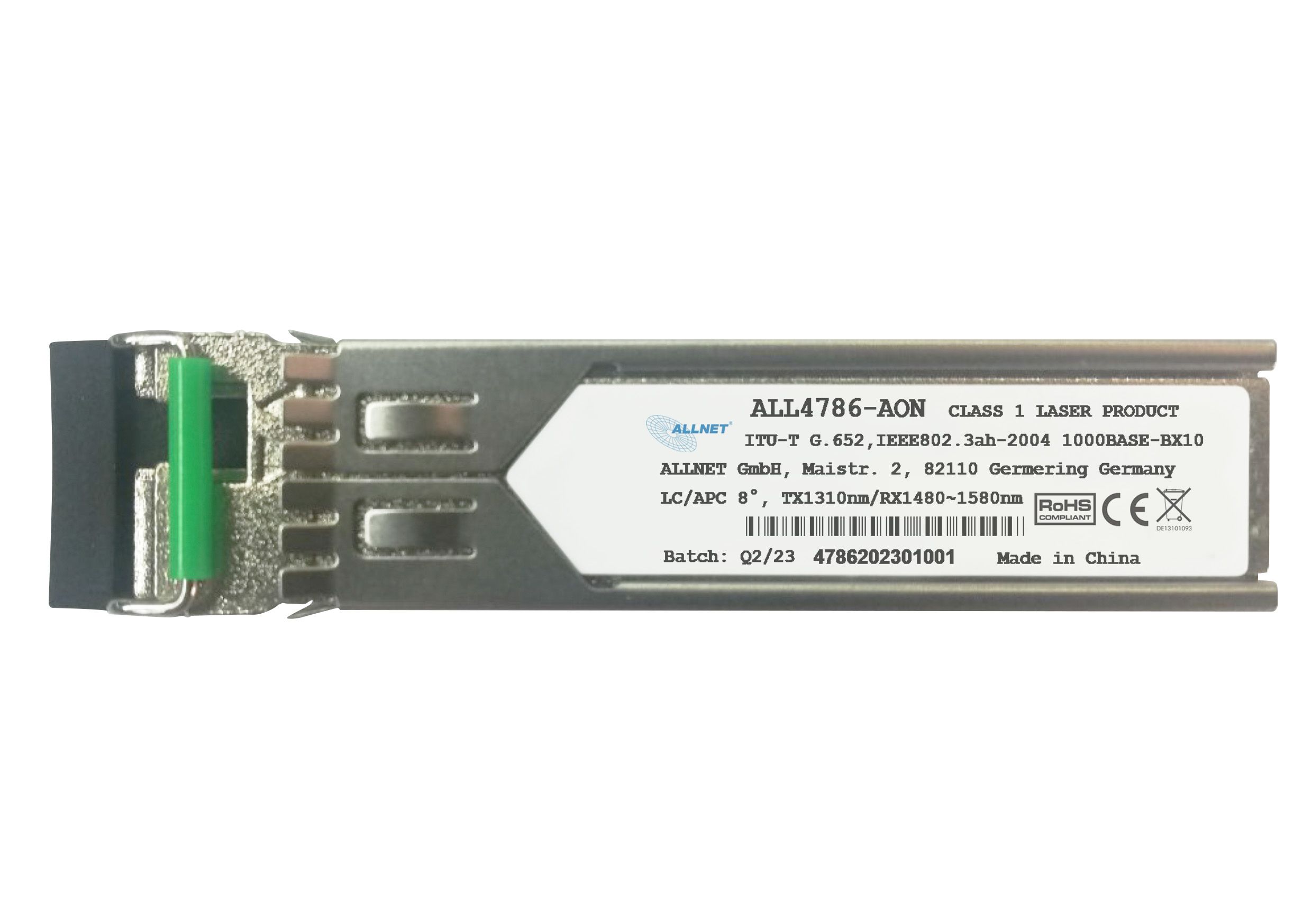
AVM FRITZ!BOX 5530 Fiber zbh. AON Replacement GBIC "ALL4786-AON"
| |||||||||||||||||||||||||||||||||||||||||||||||||||||||||||||||||||||||||||||||||||||||||||||||||||||||||||||||||||||||||||||||||||||||||||||||||||||||||||||||||||||||||||||||||||||||||||||||||||||||||||||||||||||||||||||||||||||||||||||||||||||||||||||||||||||||||||||||||||||||||||||||||||||||||||||||||||||||||||||||||||||||||||||||||||||||||||||

PART NUMBER
|
WAVE LENGTH TX/RX
|
DISTANCE
|
LASER
|
TEMPERATURE
|
ALL4786-AON
|
1310nm/1490nm
|
20km
|
FP/PIN
|
0~70?
|
Product Description
The ALLNET ALL4786-AON SFP is small form factor pluggable (SFP) transceivers compatible with multi-sourcing agreement (MSA). It is suitable for single-mode fiber (SMF) communications in 1.25Gbps Ethernet and 1G/2G Fiber Channel.
Regulatory Compliance
ALLNET ALL4786-AON transceivers are Class 1 Laser Products comply with FDA regulations. Meet Class 1 eye safety requirements of EN 60825 and the electrical safety requirements of EN 60950.
Absolute Maximum Ratings
Parameter
|
Symbol
|
Min.
|
Max.
|
Unit
|
Supply Voltage
|
VCC
|
-0.5
|
3.6
|
V
|
Storage Temperature
|
TS
|
-40
|
85
|
°C
|
Operating Case Temperature
|
TC
|
0
|
70
|
°C
|
Recommended Operating Conditions
Parameter
|
Symbol
|
Min.
|
Typical
|
Max.
|
Unit
|
Operating Case Temperature
|
TC
|
0
|
|
70
|
°C
|
Power Supply Voltage
|
VCC
|
3.15
|
3.3
|
3.45
|
V
|
Power Supply Current
|
ICC
|
|
|
300
|
mA
|
Data Rate
|
|
|
1.25
|
|
GBps
|
Max Link Length on 9/125µm SMF
|
Lmax
|
|
20
|
|
km
|
Electrical Characteristics
Parameter
|
Symbol
|
Min.
|
Typical
|
Max.
|
Unit
|
Transmitter
|
|||||
Input Differential Impedance
|
Zin
|
90
|
100
|
110
|
?
|
Data Input Swing Differential
|
Vin
|
500
|
|
2400
|
mV
|
Tx-Dis Disable
|
Vd
|
2.0
|
|
Vcc
|
V
|
Tx-Dis Enable
|
Ven
|
0
|
|
0.8
|
V
|
TX-Fault (Fault)
|
|
2.0
|
|
Vcc+0.3
|
V
|
TX-Fault (Normal)
|
|
0
|
|
0.8
|
V
|
Receiver
|
|||||
Data Output Swing Differential
|
Vout
|
370
|
|
2000
|
mV
|
Rx-Los Fault
|
Vlf
|
2.0
|
|
Vcc+0.3
|
V
|
Rx-Los Normal
|
Vln
|
0
|
|
0+0.8
|
V
|
Optical Characteristics
Parameter
|
Symbol
|
Min.
|
Typical
|
Max.
|
Unit
|
Transmitter
|
|||||
Centre Wavelength
|
?c
|
1290
|
1310
|
1330
|
nm
|
Spectral Width (RMS)
|
?
|
|
|
4
|
nm
|
Average Output Power
|
Pout
|
-9
|
|
-3
|
dBm
|
Extinction Ratio
|
ER
|
9
|
|
|
dB
|
Optical Rise/Fall Time
|
tr/tf
|
|
|
2
|
ns
|
Receiver
|
|||||
Centre Wavelength
|
?c
|
1470
|
1490
|
1610
|
nm
|
Receiver Sensitivity
|
PIN
|
|
|
-23
|
dBm
|
Receiver Overload
|
PMAX
|
-3
|
|
|
dBm
|
LOS De-Assert
|
LOSD
|
|
|
-30
|
dBm
|
LOS Assert
|
LOSA
|
-35
|
|
|
dBm
|
LOS Hysteresis
|
|
0.5
|
|
4.5
|
dB
|
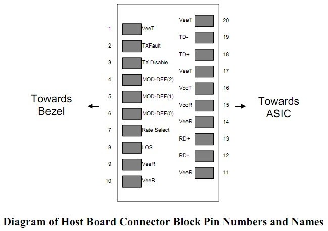
Pin Descriptions
Pin
|
Symbol
|
Description
|
Ref.
|
1
|
VEET
|
Transmitter Ground (Common with Receiver Ground)
|
6.1
|
2
|
TFAULT
|
Transmitter Fault. Not supported.
|
|
3
|
TDIS
|
Transmitter Disable. Laser output disabled on high or open.
|
6.2
|
4
|
MOD_DEF(2)
|
Module Definition 2. Data line for Serial ID.
|
6.3
|
5
|
MOD_DEF(1)
|
Module Definition 1. Clock line for Serial ID.
|
6.3
|
6
|
MOD_DEF(0)
|
Module Definition 0. Grounded within the module.
|
6.3
|
7
|
Rate Select
|
No connection required
|
|
8
|
LOS
|
Loss of Signal indication. Logic 0 indicates normal
operation.
|
6.4
|
9
|
VEER
|
Receiver Ground (Common with Transmitter Ground)
|
6.1
|
10
|
VEER
|
Receiver Ground (Common with Transmitter Ground)
|
6.1
|
11
|
VEER
|
Receiver Ground (Common with Transmitter Ground)
|
6.1
|
12
|
RD-
|
Receiver Inverted DATA out. AC Coupled.
|
|
13
|
RD+
|
Receiver Non-inverted DATA out. AC Coupled.
|
|
14
|
VEER
|
Receiver Ground (Common with Transmitter Ground)
|
6.1
|
15
|
VCCR
|
Receiver Power Supply
|
|
16
|
VCCT
|
Transmitter Power Supply
|
|
17
|
VEET
|
Transmitter Ground (Common with Receiver Ground)
|
6.1
|
18
|
TD+
|
Transmitter Non-Inverted DATA in. AC Coupled.
|
|
19
|
TD-
|
Transmitter Inverted DATA in. AC Coupled.
|
|
20
|
VEET
|
Transmitter Ground (Common with Receiver Ground)
|
6.1
|
Notes:
-
- Circuit ground is internally isolated from chassis ground.
- Laser output disabled on TDIS >2.0V or open, enabled on TDIS <0.8V.
-
- Should be pulled up with 4.7k - 10kohms on host board to a voltage between 2.0V and 3.6V. MOD_DEF(0) pulls line low to indicate module is plugged in.
- LOS is open collector output. Should be pulled up with 4.7k -10kohms on host board to a voltage between 2.0V and 3.6V. Logic 0 indicates normal operation; logic 1 indicates loss of signal.
- EEPROM & DDM THRESHOLD
-
- EEPROM
2 wire address 1010000X (A0hex)
0~95
Serial ID Defined by SFP MSA (96 bytes)
|
96~127
Vendor Speific (32 bytes)
|
128~255
Reserved (128 bytes)
|
*Customized Area
Address
|
Description
|
Hex Data
|
ASCII
|
A0 20~35
|
Vendor Name
|
41 4c 4c 4e 45 54 20 47 6d 62 48
|
ALLNET GmbH
|
-
- DDM THRESHOLD
ALL4786-AON
|
Low Alarm
|
Low Warn
|
High Warn
|
High Alarm
|
Temp
|
-5?
|
0?
|
70?
|
75?
|
Voltage
|
3V
|
3.1V
|
3.6V
|
3.7V
|
Tx Bias
|
3mA
|
4mA
|
70mA
|
75mA
|
Tx Power
|
-13.5dBm
|
-9.5dBm
|
-1dBm
|
1dBm
|
Rx Power
|
-23dBm
|
-19dBm
|
-3dBm
|
1dBm
|
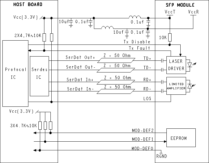
 Recommend Circuit
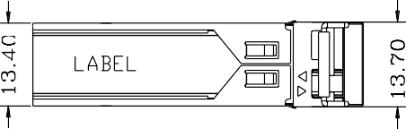
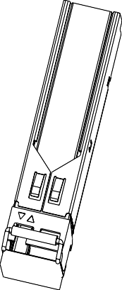
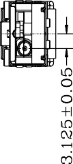
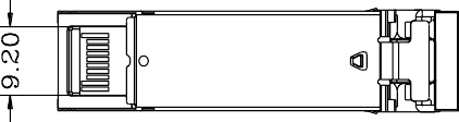
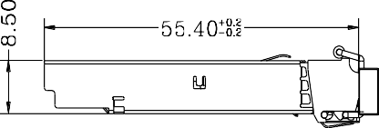 Mechanical Specifications
- Recommend Circuit
- Mechanical Specifications
![]()
![]()
![]()
![]()
![]()
![]()
![]()
![]()
![]()
![]()
![]()
![]()
![]()
![]()
![]()
![]()
Back